 Part of the Oxford Instruments Group
Expand
Collapse
Part of the Oxford Instruments Group


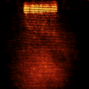
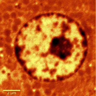
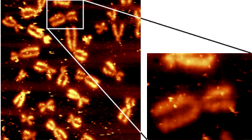
For applications requiring optical imaging beyond the diffraction limit, the witec360 microscopes can integrate a scanning near-field optical microscopy (SNOM) setup. This unique combination facilitates confocal Raman and high-resolution optical imaging, including fluorescence and luminescence analysis of the same region. This allows for efficient and comprehensive analysis of samples including cells, proteins, light-emitting devices, or waveguides.
Our Oxford Instruments SNOM technology is also available as a stand-alone microscope. Contact us for more information.
SNOM pushes the boundaries of optical imaging by exploiting the “near-field” (evanescent field) created when laser light is focused through the small aperture of a SNOM tip. Its diameter determines the optical resolution, typically 60 – 100 nm.
To generate an optical image, the sample is scanned point-by-point and line-by-line beneath the aperture. Simultaneously, a beam deflection setup similar to that used in AFM contact mode ensures that the cantilever maintains constant contact with the sample surface. This approach allows for a simultaneous acquisition of both topographical and optical data, providing a detailed view of the sample’s surface.
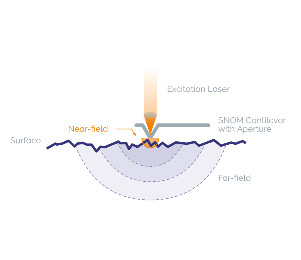
The SNOM option in witec360 microscopes operates using unique, microfabricated near-field active sensor tips and highly sensitive photon detectors. The sensor tip is magnetically held at the end of the objective’s arm, enabling simultaneous control of both the cantilever and the sample position.
Please fill in all data fields to ensure we can process your inquiry as quickly as possible.

© Oxford Instruments 2026