witec360 Raman microscope with Hexalight spectrometer launched
Take your research in any direction with the new benchmark for Raman imaging.
 Part of the Oxford Instruments Group

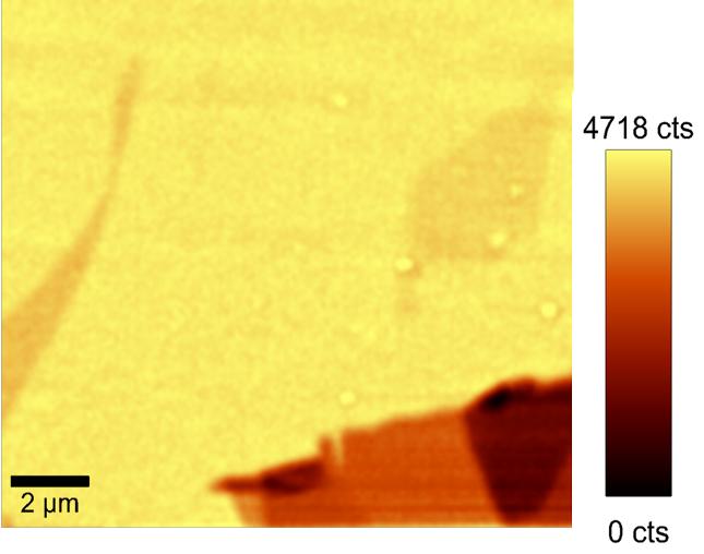
2D materials such as carbon nano-tubes, graphene or transition metal dichalcogenides (TMDs) show immense promise in many applications such as transistors, sensors, and optoelectronics. Flexible and adaptive analytical methods can support effective investigation and accelerate progress in 2D materials research and development.
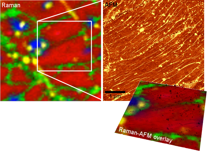
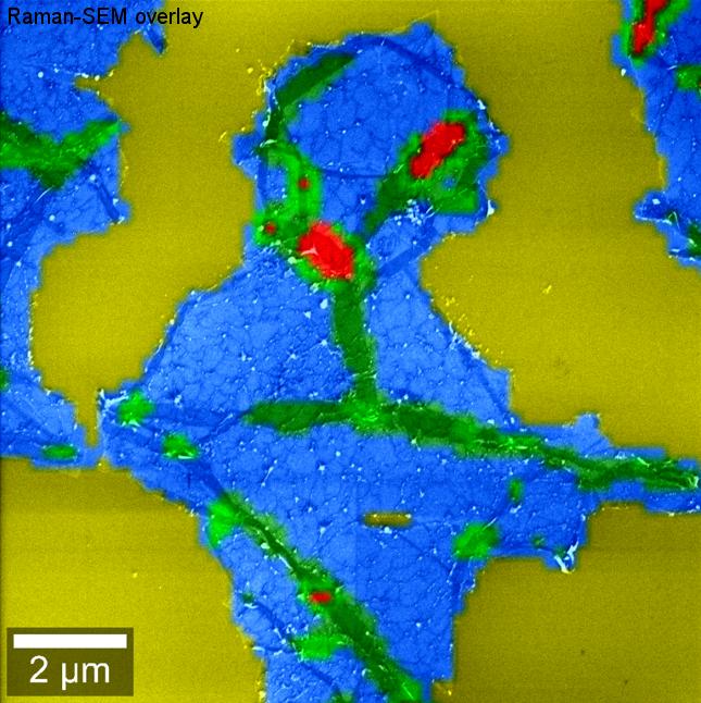
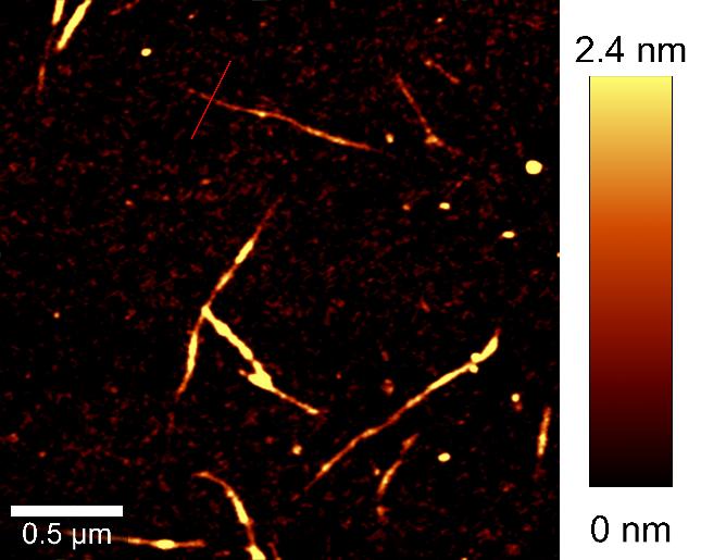
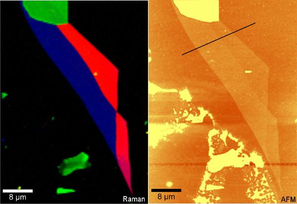
For comprehensive investigations of nano-carbon and TMD samples, Oxford Instrument witec360 Raman microscopes can be equipped with additional imaging techniques such as Atomic Force Microscopy (AFM), Scanning Near-field Optical Microscopy (SNOM) and Scanning Electron Microscopy (SEM). All provided imaging techniques can be fully integrated in a single device.
Application Note -
Correlative Imaging of 2D Material Heterostructures: Raman, PL and SHG
Application Note 2D Materials
Application Note Raman-SEM (RISE) Imaging
Application Note Correlative Imaging of MoS2
Application Note cryoRaman
If you'd like to learn more about the possibilities of Raman imaging for your individual field of application, one of our specialists will be happy to discuss them with you.
Contact us
© Oxford Instruments 2026