Related Articles
- What is confocal Raman microscopy?
- Does the excitation wavelength influence the measurement?
- What is the spectral resolution?
What is the spectral resolution?
Spectral resolution is the ability of a spectroscopic system to separate adjacent peaks. Confocal Raman systems have a spectral resolution which is primarily defined by:
- The focal length of the spectrometer (the longer the focal length, the higher the spectral resolution)
- The grating (the higher the groove density, the higher the spectral resolution)
- The pixel size on the CCD camera (the smaller the pixels, the higher the spectral resolution)
- The entrance slit or pinhole (the smaller the slit/pinhole the higher the spectral resolution)
- The line shape preservation (=imaging quality) of the spectrometer
The spectral resolution can be experimentally determined e.g. by measuring the peak resolution on known reference samples. An established sample used to demonstrate spectral resolution is for example CCl4.
With few exceptions the natural linewidths of Raman lines are typically larger than 3 cm-1. Therefore a spectral resolution in the range of 1 cm-1 is sufficient for the majority of samples.
Related Articles
What is the Raman effect and what is Raman scattering?
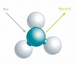
Raman effect:
The Raman effect was first experimentally discovered and described by the physicist Chandrasekhara Venkata Raman (* 1888, † 1970) in 1928. The Raman effect is based on inelastic light scattering at the chemical bonds of a sample. Due to vibrations in the chemical bonds this interaction causes a specific energy shift in parts of the back scattered light which results in a unique Raman spectrum.
Raman scattering:
Raman scattering is a very weak effect, typically less than one in a million excitation photons give rise to a single Raman photon. Raman scattering can be further differentiated as Stokes and Anti-Stokes scattering. Both contain information about the material and its molecular composition.
- Stokes scattering: The photon transfers energy to the molecule. The emitted photon has a lower energy than the absorbed photon.
- Anti-Stokes scattering: The molecule transfers energy to the photon. The emitted photon has a higher energy than the absorbed photon.
In addition to inelastic scattering, elastic scattering can also appear. Elastic scattering at the same energy as the incident radiation is called Rayleigh scattering. It does not contain any information about the molecules and cannot be used for chemical sample analysis in a confocal Raman microscope.
Related Articles
What kind of Information is contained in the Raman spectrum?
A Raman spectrum is the unique fingerprint of a material. It can provide qualitative and quantitative information.
The bands shifted to higher wavenumbers (blue shifted) are called anti-Stokes Raman bands and those shifted to lower wavenumbers (red shifted) are called Stokes Raman bands. Usually, the intensities of the Stokes-shifted Raman bands are more intense and therefore used for qualitative and quantitative analysis.
In addition to the chemical compound distribution, there are further properties that can be derived from the Raman spectrum:
- The peak intensity gives information about the quantity of a specific compound
- A peak shift can identify stress and strain states
- The peak width reveals the degree of crystallinity
- The polarization state provides information regarding crystal symmetry and orientation

Related Articles
- What is the Raman effect and what is Raman scattering?
- How should one perform polarization dependent measurements?
- What are low-wavenumber measurements?
The Raman Technique
What is confocal Raman imaging?
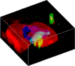
3D confocal Raman image of a fluid inclusion in garnet. The different colors represent different molecular phases.
For confocal Raman imaging a confocal Raman microscope scans the sample point-by-point and line-by-line, and at every image pixel a complete Raman spectrum is acquired. This process is also called hyperspectral imaging. The acquired multi-spectrum files contain the information of thousands to millions of Raman spectra. These files are analyzed with software to generate an image that displays the spatial distribution of the chemical components. By taking a stack of images at different focal positions (in the z-direction), 3D images can be created.
What are the sample requirements for Raman analyses?
Raman analyses can be performed on a variety of samples such as gases, liquids, powders and solids. Only pure metals may cause difficulties due to the fact that they are Raman-inactive.
In general, there is no sample preparation (such as dyeing or dissection) required and Raman spectroscopic measurements can be performed in situ, in vitro, and in vivo.
The maximum applicable sample size for Raman imaging is dependent on the Raman microscope capabilities and the maximum scan range is dependent on the integrated scan stage. Typically, sample areas from 200 x 200 µm² up to 50 x 50 mm² can be investigated. In case of sufficiently transparent sample depth scans in the z-direction are also possible.
Does the excitation wavelength influence the measurement?
The wavelength has a strong effect on the measurement outcome and the obtainable information. It influences:
- The Raman signal: The Raman scattering intensity is proportional to ν 4, where ν is the frequency of the excitation laser radiation, i.e. lower excitation wavelength lead to higher Raman signals.
- The fluorescence signal: Many samples show strong fluorescence when excited in the UV or blue region and low fluorescence when excited in the red or NIR region of the spectrum. The fluorescence signal is comparatively strong and could obscure the weaker Raman signal.
- The spatial resolution: The shorter the excitation wavelength, the higher the spatial resolution. Caution: For the spatial resolution, the NA of the objective should also be considered.
- The sample damage: For short wavelengths the high photon energy may cause sample damage at a lower laser power than for longer wavelengths.
Which lasers are suitable for Raman analyses?
A laser suitable for Raman microscopy has the following characteristics:
- Gaussian beam shape (single longitudinal mode TEM00), so that it can be focused onto a diffraction-limited spot
- a narrow line shape of well below 1 cm-1, to avoid broadening of the Raman lines
- very stable in frequency (variations < 0.01 cm-1), to allow stress measurements with high accuracy
- very stable in intensity (< 1-2 % power fluctuations), to allow accurate and comparable measurements of concentrations
- linear polarization, to allow the observation of polarization-dependent sample properties
Related Articles
- What are the sample requirements for Raman analyses?
- Does the excitation wavelength influence the measurement?
- Which is the right objective for my experiments?
The Microscope
What is confocal microscopy?
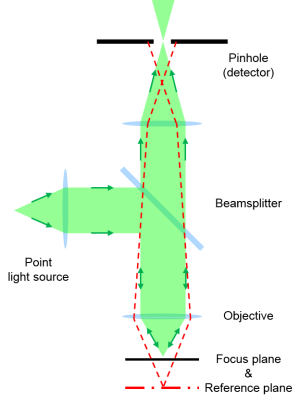
Principle of confocal microscopy.
The aim of confocal microscopy is the suppression of light from out-of-focus planes. This is realized firstly by a point illumination in the focal plane and secondly by a pinhole in the conjugate plane of the detection beam path.
Due to the point illumination and detection only information from a single point is determined at a time. In order to generate an image the sample is scanned point-by-point and line-by-line.
The advantages of confocal microscopy over conventional wide-field microscopy are an improved resolution in the lateral plane, a high discriminatory power in axial direction, a reduced background signal, and the opportunity to collect serial optical sections from different focal planes to generate depth profiles or 3D images.
Related Articles
Why is the pinhole size important?
The pinhole size is a compromise between resolution and signal throughput. On the one hand the signal should be as high as possible, while on the other hand the spatial resolution should be as good as possible. A small pinhole strongly increases the depth and also the lateral resolution. However, the signal that reaches the detector is decreased.
What is confocal Raman microscopy?
The confocal Raman imaging technique combines Raman spectroscopy with a confocal microscope by acquiring the information of a complete Raman spectrum at every image pixel. Thus the spatial distribution of the chemical components within the sample is detected and imaged. High-resolution confocal Raman microscopes achieve a lateral resolution at the diffraction limit (~ λ/(2NA); typically 250 – 300 nm for 532 nm excitation wavelength and 100x 0.9 NA objective). A confocal microscope setup is furthermore characterized by an excellent depth resolution (below 1 µm) and allows the generation of 3D Raman images and depth profiles.
What influences the throughput of a confocal Raman microscope?
The throughput of a confocal Raman microscope has a direct impact on the amount of time needed for confocal Raman imaging and the sensitivity and capability of the system. It is influenced by various microscope components, such as the objective, coupling elements and filters, the pinhole, the spectrometer, and the CCD camera. To optimize the throughput, every part of the system must be optimized for the highest transmission and efficiency.
| high-throughput system | low-throughput system |
| high quality objective | low quality objective |
| beam guidance using a single fiber | beam guidance using mirrors (e.g. 3 mirrors) |
| lens-based spectrometer | mirror-based spectrometer |
| back-illuminated CCD camera | front-illuminated CCD camera |
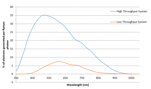
High-throughput system optimized for 532 nm excitation wavelength vs. low-throughput system. Throughput limitations due to the pinhole are neglected for both cases.
Which is the right objective for my experiments?
When selecting the right objective, all measurement conditions should be taken in consideration. A good microscope objective may have 80-90% transmission at 500 nm wavelength, but only 40% or less at 900 nm. The working distance between sample and objective and the opportunity to measure under specific conditions such as low-temperatures or in liquids are also important factors in that decision. Furthermore the correction of imaging errors, e.g. chromatic aberrations, is an important quality characteristic.
More than the magnification, the numerical aperture (NA) plays a crucial role: The highest collection efficiency and the best spatial resolution can be obtained by using an objective with the highest NA applicable under the measurement conditions. The NA additionally defines the resolving power and the power density of the excitation spot. However, a lower NA can be beneficial if the sample’s topography requires a broader collection range in the z-direction.
Related Articles
- What influences the throughput of a confocal Raman microscope?
- How is the spatial resolution defined?
What are the characteristics of fiber-coupled Raman systems?
Fiber-coupled microscope systems use single mode optical fibers to deliver light from the laser to the microscope. The transmitted light maintains a TEM00 mode and preserves its Gaussian character independently of the laser power attenuation, thus allowing diffraction limited resolution.
Multi-mode optical fibers in the detection beam path enable the transmission of up to 90% of the Raman signal. For comparison, an Al-mirror based optical system using three mirrors achieves only about 78% efficiency in light transmission at 532 nm excitation wavelength. If the number of mirrors used increases, the light transmission efficiency drops further. Therefore the usage of optical fibers is particularly apt for ultrahigh-throughput microscope systems.
Related Articles
- What influences the throughput of a confocal Raman microscope?
- Which lasers are suitable for Raman analyses?
- What are the differences between mirror-based and lens-based spectroscopic systems?
The Spectroscopic System
What are the differences between mirror-based and lens-based spectroscopic systems?
Mirror-based spectrographs have aspherical or toroidal mirrors that guide the light from the entrance slit to the grating and on to the detector. Typically a minimum of two or three mirrors are used per spectrograph. Mirror-based spectrometers cover a wide spectral range and therefore a single spectrometer can be used with several excitation wavelengths. However, the imaging quality of mirror-based spectrometers is rather poor due to aberrations that can be introduced from the mirrors leading to distortions on the CCD detector. Also the light transmission rate of a mirror-based spectrometer is commonly only around 45 %. Due to these factors mirror-based spectrometers are typically used for the detection of single Raman spectra and strong Raman scatterer, but are not ideal for the fast generation of Raman images and the detection of weak Raman signals.
Lens-based spectrographs use an on-axis lens-system instead of mirrors to guide light through the spectrometer. The lenses are optimized for a certain spectral range and can therefore provide optimal Raman signal transmission (typically as high as 60 - 70%), spectral resolution and imaging capability. Therefore lens-based spectrometers are the preferred spectroscopic system for the generation of high-quality Raman images.
How does the grating influence the measurement?
The grating in a spectrometer disperses the signal onto the CCD detector by deflecting each wavelength at a different angle. The number of grooves per millimeter determines the dispersion characteristics. A high number of grooves/mm (lines/mm) results in a high dispersion and thus a high resolution, by distributing the signal over a larger number of CCD pixels.
To optimize efficiency, gratings are typically “blazed” for a certain wavelength. This means that the grooves are angled so that the grating efficiency can reach 80% for the first diffraction order. The grating efficiency sets the upper limit of the throughput of the spectrometer.
It is often useful to switch between multiple gratings: one that covers the full Raman spectrum (-100 to 3600 cm-1) and a high-resolution grating that delivers approximately 1 cm-1 spectral resolution.
Which CCD detectors can be used?
The CCD (charged-coupled device) camera is the last element in the detection beam path and converts the photons that reach the chip into electrons and then a signal that can be used in the software. The CCD camera is an important component of a Raman microscope and choosing the correct CCD strongly affects the performance of the instrument. The quantum efficiency (QE) is a key element of these cameras. QE is the percentage of detected photons out of the total of incoming photons. The figure below shows the room-temperature QE-curves of three typical cameras.
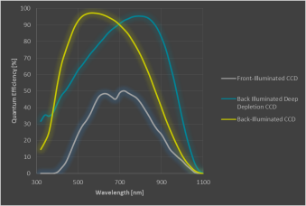
Example Quantum Efficiencies of commonly used CCDs.
The following CCDs are commonly used for Raman spectroscopy:
- In the visible range, the back-illuminated CCD camera is the camera of choice. It has a high QE and increases the instrument throughput.
- Front-Illuminated CCDs do have a broader operating range but with a low QE compared to back-illuminated CCDs. They also show a very low dark noise.
- For detecting wavelengths longer than approximately 850-900nm, deep-depletion CCD cameras are the best choice as they have a NIR-optimized coating and the best QE in this range. This type of camera shows a higher dark noise than the ones mentioned previously.
- Back-Illuminated EMCCDs (electron multiplying CCD) are currently the most sensitive spectroscopic detectors on the market with a total amplification of the signal of up to 1000x. Thus ultra-fast Raman imaging can be performed (acquisition of ca. 1300 spectra per second).
Related Articles
Advanced Raman Techniques and Combinations
What is Resonance Raman?
In Resonance Raman (RR) scattering the excitation wavelength is chosen to fall within an absorption band of the molecule under investigation. This can lead to an increased intensity of the Raman signal and an improved signal-to-noise ratio. RR has some more advantages: First, only those modes that are coupled to the electronic excitation are resonantly enhanced, which leads to a drastic reduction of the spectral complexity. Second, RR can be used to selectively investigate a specific analyte in a mixture by tuning the excitation wavelength to the absorption band of the particular analyte. A disadvantage of RR is that not only inelastically scattered light but also increased fluorescence and luminescence is observed.
What is Surface-Enhanced Raman Spectroscopy (SERS)?
Surface-Enhanced Raman Scattering was first observed by Fleischmann et al. in 1974. The principle is that noble metal nanoparticles in close proximity to the measurement position enhances the Raman scattering. At the same time the complexity of the Raman spectrum is typically reduced to prominent marker bands. SERS has been documented for molecules adsorbed on metallic structures formed of, e.g. silver, gold, aluminum, copper, palladium, and platinum, and a correlation between the surface roughness of the metallic structure and the SERS enhancement has been established. Commercially available SERS substrates now provide a reliable and efficient source to perform SERS experiments.
SERS can be coupled with Resonance Raman by using a laser excitation wavelength in resonance with the molecular energy levels (Surface-Enhanced Resonance Raman Scattering (SERRS)).
What is Tip-Enhanced Raman Spectroscopy (TERS)?
Tip-Enhanced Raman Spectroscopy (TERS) enables the acquisition of chemical information with a lateral resolution far below the diffraction limit. The TERS measurement technique is a combination of surface-enhanced Raman scattering (SERS) with scanning probe microscopy (SPM) techniques such as Atomic Force Microscopy (AFM). Thus it combines the high spatial resolution of AFM with the chemical sensitivity of Raman scattering.
To obtain the TERS effect a metal coated AFM-tip can be used as a nanostructure. The excitation laser light is focused onto the tip-apex to enhance the Raman signal in close proximity to the tip. The lateral resolution is thereby dependent on the tip-apex size (10 – 20 nm). The TERS effect is assumed to be based on surface plasmons and chemical resonance effects resulting in enhanced electrical fields and increased Raman signal intensities. The TERS tip illumination is usually applied from either above, below or from the side.
Although TERS is drawing more and more attention, its practical fields of application are limited to a few samples and scientific questions. Also the availability of commercial TERS-tips is still not established. Furthermore the cost of the metal-coated tips increases the total expense for the experiments to a significant degree.
TERS application examples can be found in the following publications:
How should one perform polarization dependent measurements?
Polarization dependent measurements allow the investigation of polarization dependent activity of specific peaks in a Raman spectrum. This can be used to analyze molecular orientations and geometries of e.g. crystal lattices, liquid crystals, amorphous materials, or polymers.
Therefor the polarization of the excitation light can be rotated in different angles in the focal plane (e.g. parallel, perpendicular, circular, etc.) and the Raman scattered light can then be analyzed in any orientation relatively to the polarization direction of the excitation light.
What are low-wavenumber measurements?
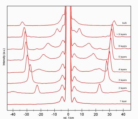
Low-wavenumber Raman spectra of different MoS2 layers.
Most spectroscopic systems allow the analysis of wavenumbers down to 100 – 200 cm-1. Low-wavenumber measurements provide additional spectral information from Stokes and Anti-Stokes Raman signals close to the Rayleigh line. Therefore a specific coupler is integrated with the microscope setup which allows the acquisition of Raman spectra at wavenumbers down to below 10 cm-1. Low wavenumber measurements are often applied to the investigation of poylmorphs in pharmaceutical research, polymer research, semiconductor research, nano-carbon research and the investigation of crystallinity.
Publication regarding low-wavenumber measurements in graphene research:
Information about low-wavenumber measurements with Oxford Instruments RayShield Coupler
Related Articles
What is topographic confocal Raman imaging?
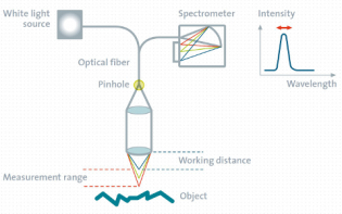
Topographic confocal Raman imaging enables 3D chemical characterization on rough, inclined or irregularly-shaped samples and can be carried out precisely along or at a set distance from a surface without requiring sample preparation.
The topographic sensor operates according to the confocal chromatic sensor principle: A white-light point source is focused onto the sample with a lens system that has a strong linear chromatic error (hyperchromatic lens system). Every color has therefore a different focal distance. The light reflected from the sample is focused through a pinhole onto a dedicated spectrometer on top of the sensor. As only one specific color is in focus at the sample surface, only this light can pass through a confocal pinhole. The detected wavelength is therefore directly related to the surface topography.
Scanning the sample in the x-y-plane reveals a topographic map of the sample. With this map the sample's surface can be kept in focus during the entire measurement procedure, irrespective of its topography.
The optical sensor controls the distance between the objective and the sample surface with sub-micrometer precision. Thus, any variation occurring during measurements with long integration times is compensated for, resulting in sharp and detailed images.
Information about TrueSurface Microscopy for topographic Raman imaging
What is ultrafast confocal Raman imaging?
Using an EMCCD detector, ultrafast confocal Raman imaging can be performed. The acquisition time for a single Raman spectrum can be as low as 760 microseconds and 1300 Raman spectra can be acquired per minute. As a confocal Raman image typically consists of tens of thousands of spectra, the new option reduces the total acquisition time for a complete image to only a few minutes. For example, a complete hyperspectral image consisting of 250 x 250 pixels = 62,500 Raman spectra can be recorded in less than a minute.
Ultrafast Raman imaging is particularly suitable for large-area confocal Raman images due to the drastic reduction in measurement time. Delicate and sensitive samples such as living organism also benefit from the reduced measurement time and the low level of excitation power necessary.
What is near-field Raman imaging?
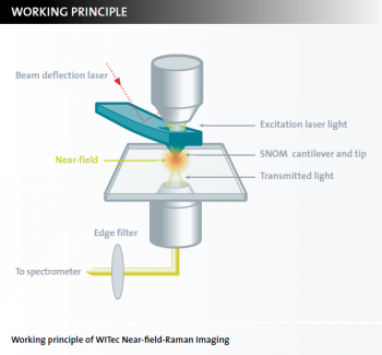
Near-field Raman Imaging is a combined microscopy technique that links chemical Raman information to high resolution Scanning Near-field Optical Microscopy (SNOM). It allows the acquisition of high-resolution confocal Raman images. Lateral resolutions of down to 60 nm can be achieved.
The near-field Raman imaging principle
The excitation laser light is focused through the SNOM-tip resulting in an evanescent field (near-field) on the far side of the aperture. While the sample is moved on a piezo-driven scan stage, the transmitted light is spectroscopically detected point by point and line by line in order to generate a hyperspectral image. The optical resolution of the transmitted light is limited only by the diameter of the aperture (down to 60 nm). Using a beam deflection setup as in AFM contact mode, it is ensured that the cantilever is always in contact with the sample. In this way the topography is recorded simultaneously along with the Near-field Raman measurement.
What possible Raman combinations are there?
Confocal Raman imaging is a non-destructive imaging technique and can therefore be combined with other techniques.
By investigating a sample with different imaging techniques the diverse information contained within the results contribute to a more comprehensive sample analysis. Furthermore the advantages of both imaging techniques can be combined to increase resolution.
Here are some examples of common Raman combinations:
Raman and AFM
By combining confocal Raman imaging with AFM, the chemical properties of the sample can be easily linked with the surface structure and mechanical properties. These two complementary techniques are available in combined Raman-AFM microscopes for more flexible and comprehensive sample characterization.
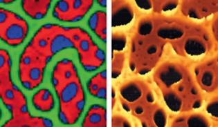
Raman and AFM image from the same sample area of a polymer blend.
Raman and SNOM
Combining Raman with SNOM (Scanning Near-field Optical Microscopy) links chemical characterization to optical imaging below the diffraction limit. If the Raman measurements are performed through the SNOM tip, high-resolution images with a lateral resolution down to 60 nm can be generated.
Raman and SEM
The Raman-SEM combination is a new correlative microscopy technique. Structures in the nm-range detected by SEM can now be correlated to chemical Raman imaging from the same sample area.
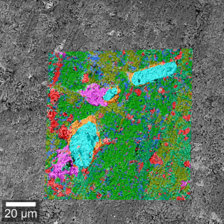
SEM image with inlay of the Raman image of a rock sample.
Information about the Raman Imaging and Scanning Electron Microscope RISE


