witec360 Raman microscope with Hexalight spectrometer launched
Take your research in any direction with the new benchmark for Raman imaging.
 Part of the Oxford Instruments Group

Materials science plays a vital role in understanding and improving the materials that shape our industries, technologies, and everyday lives. Whether you are developing cutting-edge polymers for advanced applications, ensuring the structural integrity of semiconductors, or preserving the legacy of historic artifacts, understanding the chemical, structural, and physical properties of materials is essential.
Our Raman microscopes empower scientists to uncover these insights with precision and detail. They deliver a non-invasive, highly sensitive analytical approach to visualize molecular composition, detect impurities and defects, resolve structural alignment, and study intrinsic or extrinsic stresses – advancing discoveries and driving technological progress.
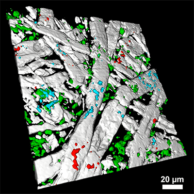
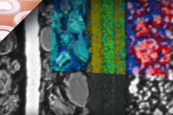
For users in manufacturing and quality control, the Oxford Instruments Raman microscopes offer a non-destructive and versatile solution for analyzing material composition and quality. With class-leading depth resolution and confocality, our instruments precisely resolve individual structures and localize defects, even beneath the surface.
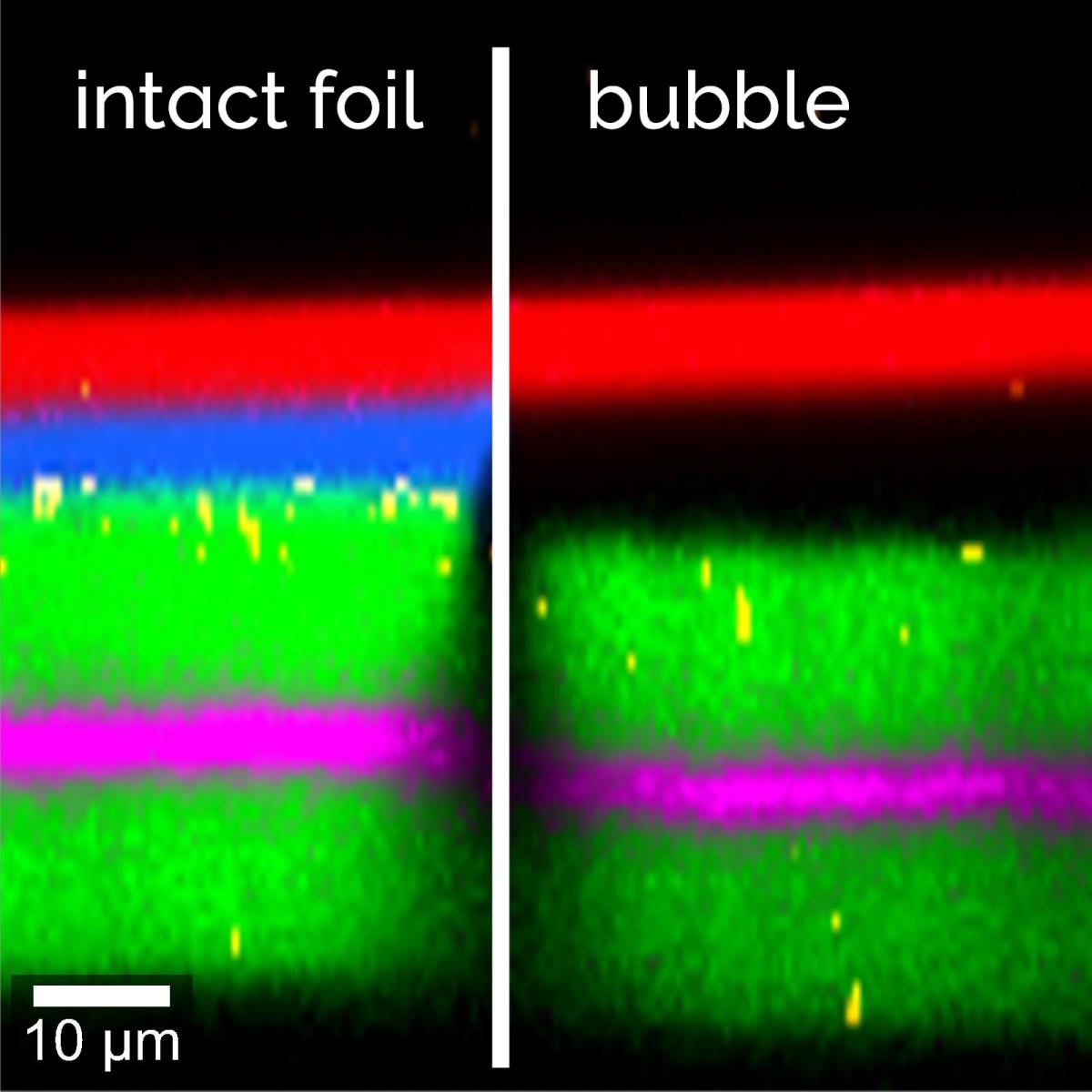
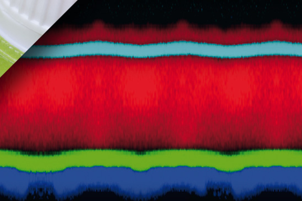
In the example shown, a Raman depth scan of a plastic foil identified a defect causing an air bubble inclusion. The analysis revealed that the glue layer binding the polyester and polyethylene layers was missing.
Understanding how materials respond to external stimuli is crucial for predicting their performance and stability. Raman microscopy enables in-situ and in-operando measurements, allowing researchers to observe materials under real-world conditions without influencing their behavior.
Our witec360 microscopes offer exceptional flexibility, with the ability to integrate custom sample holders and devices tailored to your specific application. This makes them ideal for studying thermal, chemical, or mechanical influences in real-time.
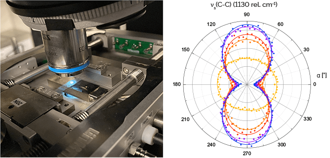
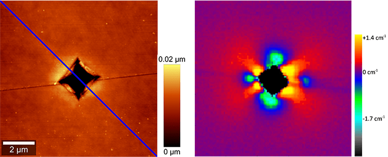
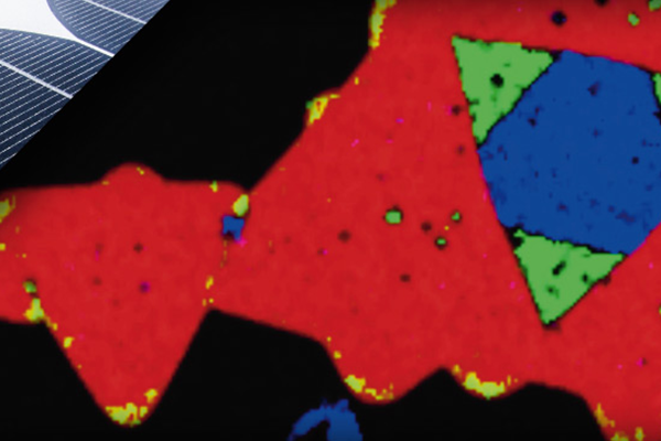
With the exceptional sensitivity of our Raman microscopes, material scientists can efficiently detect compressive and tensile stress fields in crystalline materials. This capability enables the evaluation of mechanical properties and the assessment of potential risks of material failure.
In the example shown, Raman and AFM images visualize material deformation and stress fields in silicon after a Vickers test.
Read more about Raman stress analyses in our Application Note on Correlative Raman Imaging of Semiconducting Materials.
Combine Raman microscopy with complementary material analysis techniques to gain multidimensional insights into your samples and learn about their chemical, structural, optical, physical and topographical characteristics.
Oxford Instruments Raman microscopes can seamlessly integrate:
Learn more about the possibilities for your application in our Application Notes.
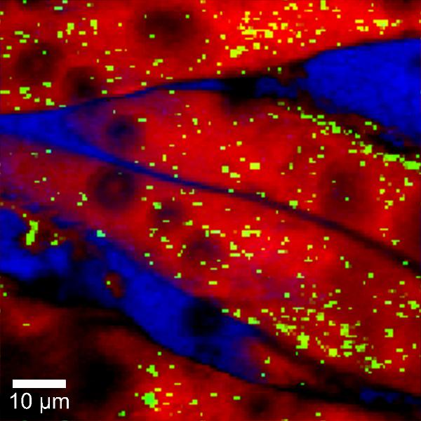
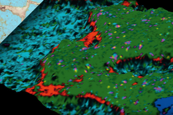
ParticleScout streamlines particle analysis by enabling rapid surveying, classification, quantification, and identification of particles. It offers an optimized Raman measurement mode for users interested in contamination, particle morphology, and particle distribution in various samples.
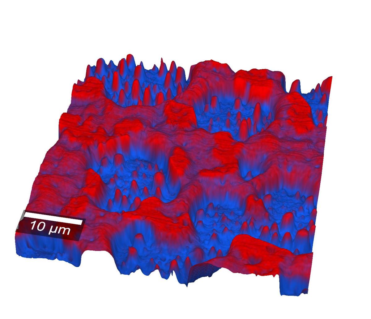
Discover ParticleScoutTrueSurface advances confocal Raman imaging by correcting for the sample’s topography within the measurement process. This feature ensures accurate characterization of uneven or irregular surfaces, making it ideal for investigating complex surfaces in material sciences.
Discover TrueSurfaceFor institutions with multiple users or those operating under strict compliance regulations, we provide tailored solutions to ensure regulated user access, streamlined workflows, and consistent results across all measurements.

If you'd like to learn more about the possibilities of Raman imaging for materials science applications, one of our specialists will be happy to discuss them with you.
Contact us
© Oxford Instruments 2026