Part of the Oxford Instruments Group
Expand
Collapse
Part of the Oxford Instruments Group

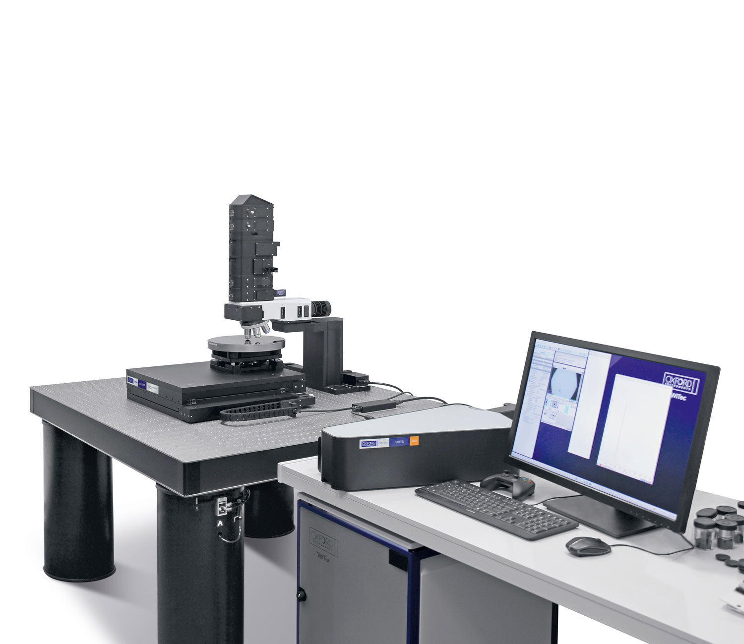
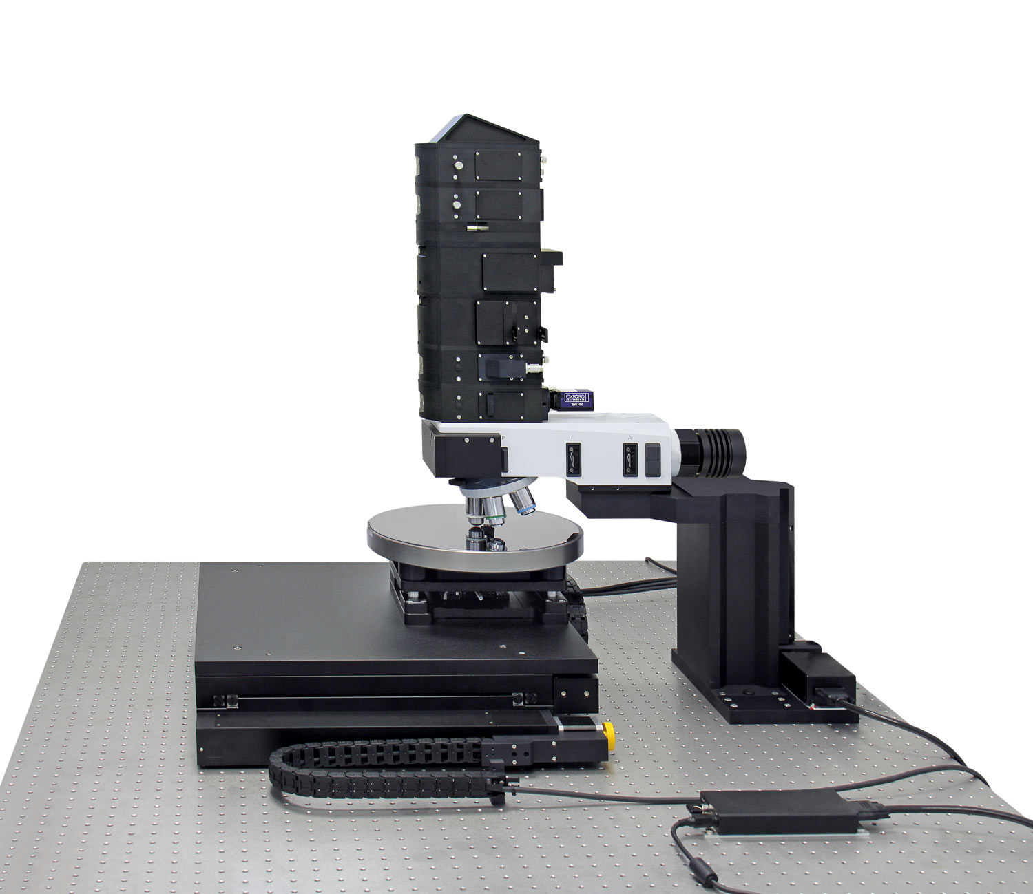
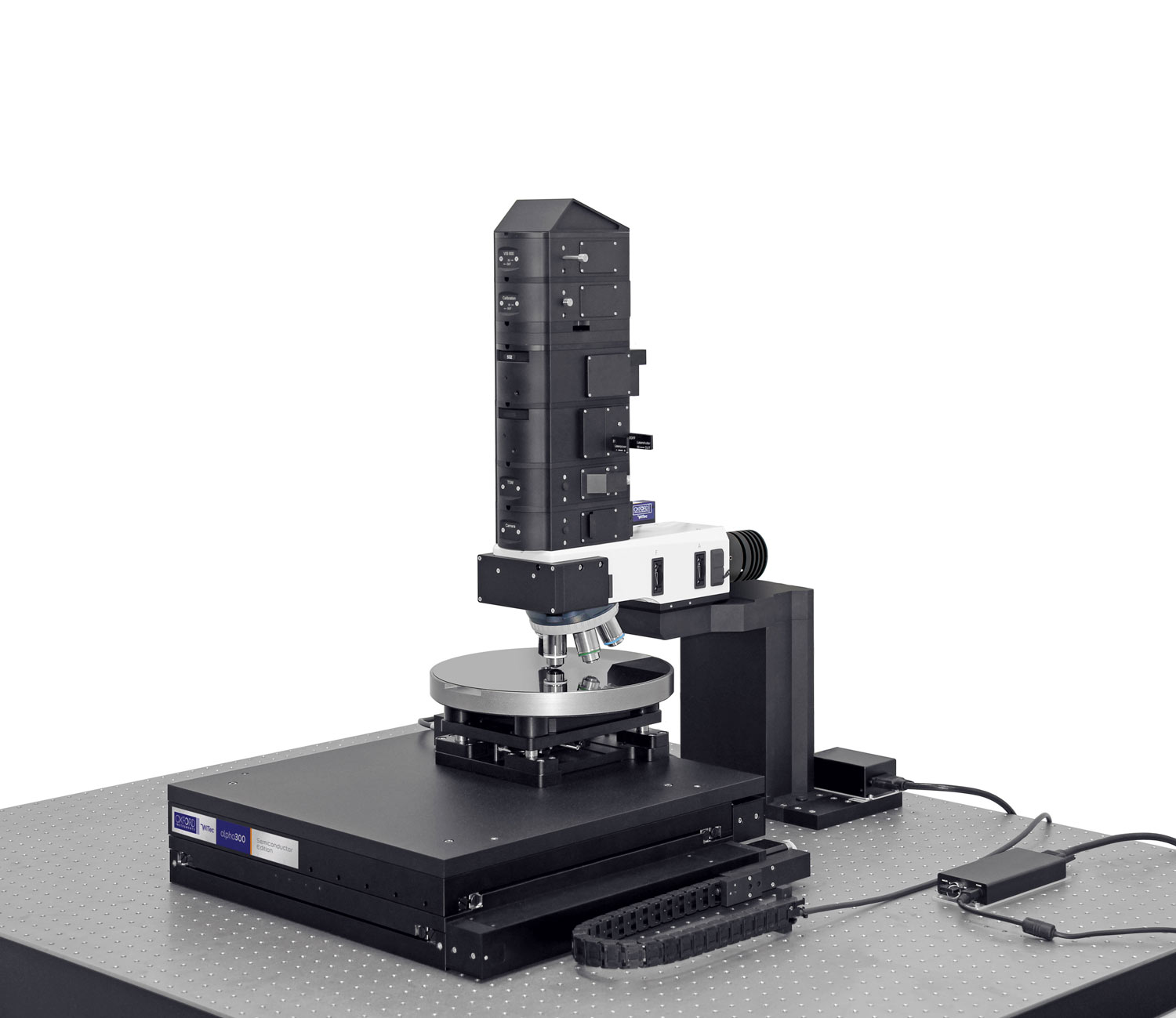
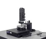
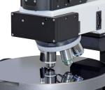
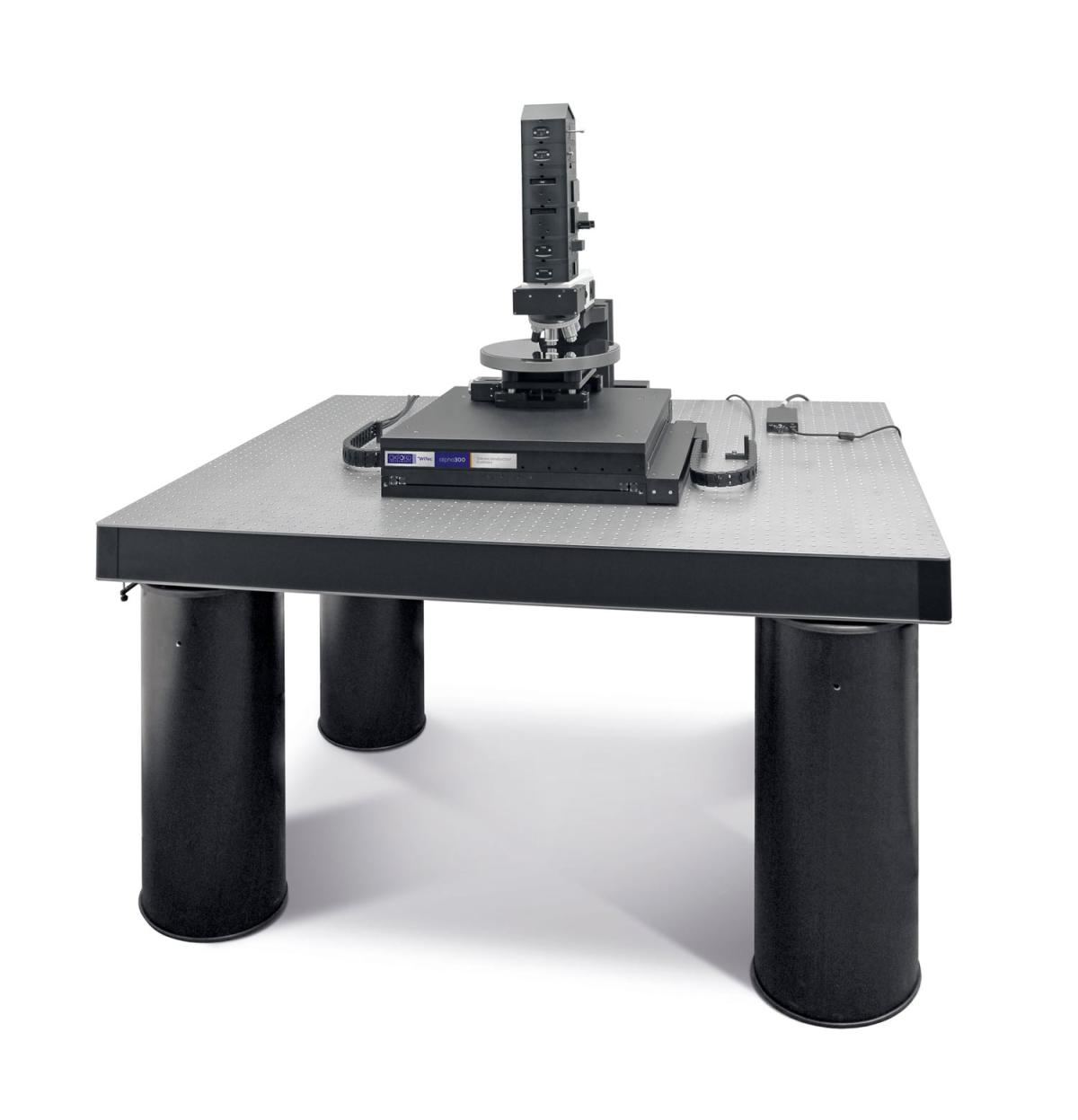
The witec360 Semiconductor Edition is a high-end confocal Raman and photoluminescence (PL) microscope specifically configured for the chemical imaging of semiconducting materials. It helps researchers accelerate the characterization of crystal quality, strain and doping in their semiconductor samples and wafers.
The microscope’s extended-range scanning stage enables the inspection of up to 12 inch (300 mm) wafers and the acquisition of large-area Raman images. It is equipped with vibration damping and active focus stabilization to compensate for topographic variation during measurements over large areas or long acquisition times. All microscope components are fully automated, permitting remote-control and the implementation of standard measurement procedures.
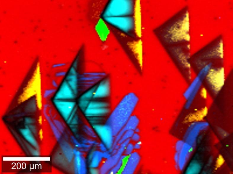
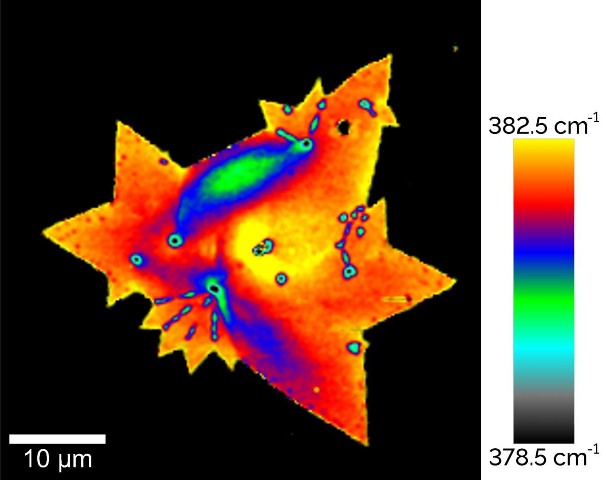
Raman imaging is able to distinguish polymorphs and characterize crystal defects below the sample’s surface. This 3D Raman image reveals the origin of a defect in a 4H-SiC wafer and identifies it as the 3C-SiC polymorph. Read more in our application note: Correlative Raman Imaging of Compound Semiconductors
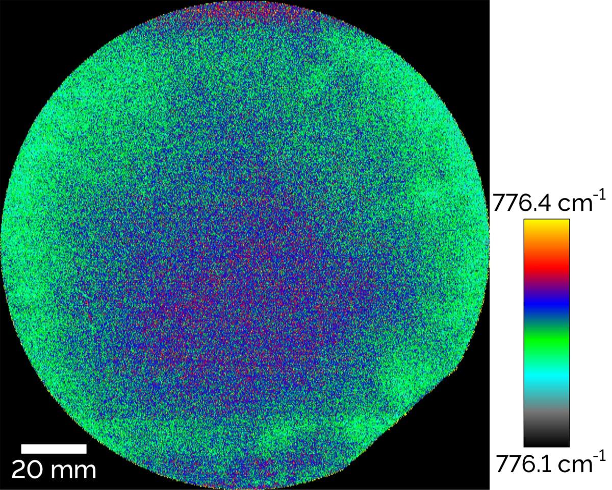
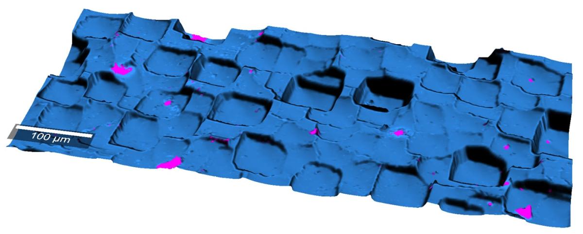
Monitoring the quality of wafers is critically important for the semiconductor industry. In order to establish the homogeneity of the material and reveal areas of strain or inhomogeneous doping, the entire area of a wafer must be investigated.
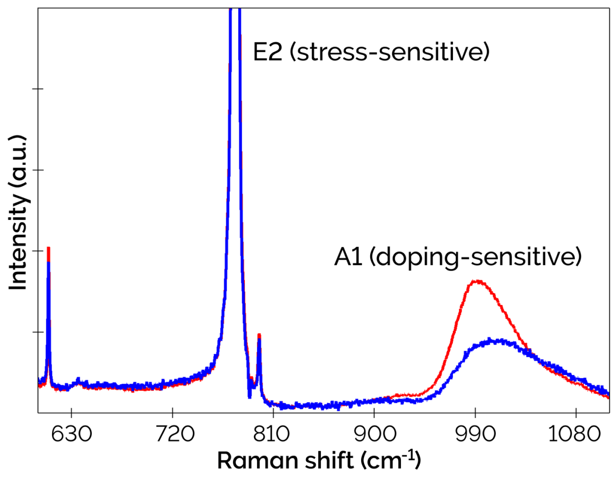
In this example, the complete surface of a 150 mm (6 inch) silicon carbide (SiC) wafer was imaged with Raman microscopy using a 532 nm laser for excitation. The analysis showed that the doping concentration was not homogeneous over the full area. The microscope‘s highly sensitive spectrometer was able to detect peak shifts below 0.01 cm-1 and could thus reveal stress fields within the wafer.
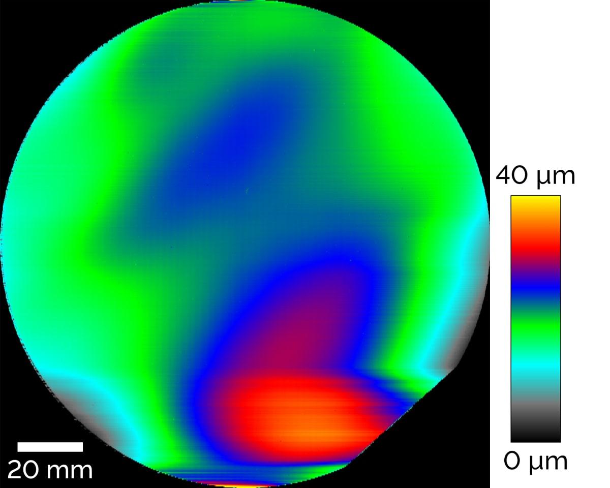
To obtain a sharp Raman image of the entire wafer, actively keeping the surface in focus was crucial. TrueSurface recorded the wafer’s topography simultaneously with the Raman data and compensated for height variations.
Read more in our application note: Correlative Raman Imaging of Compound Semiconductors
Sample courtesy of the Fraunhofer Institute for Integrated Systems and Device Technology IISB, Erlangen, Germany.
In order to meet your individual requirements, we offer a set of microscope configuration packages for the witec360 Semiconductor Edition. Whether you investigate compound semiconductors, layered structures, wide-bandgap semiconductors or 2D materials, you can choose the configuration package that best suits your research. Our specialists will be happy to discuss the right instrument for you.
Contact us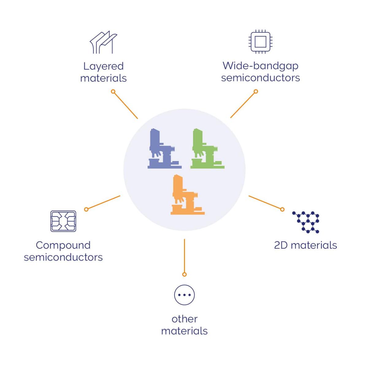
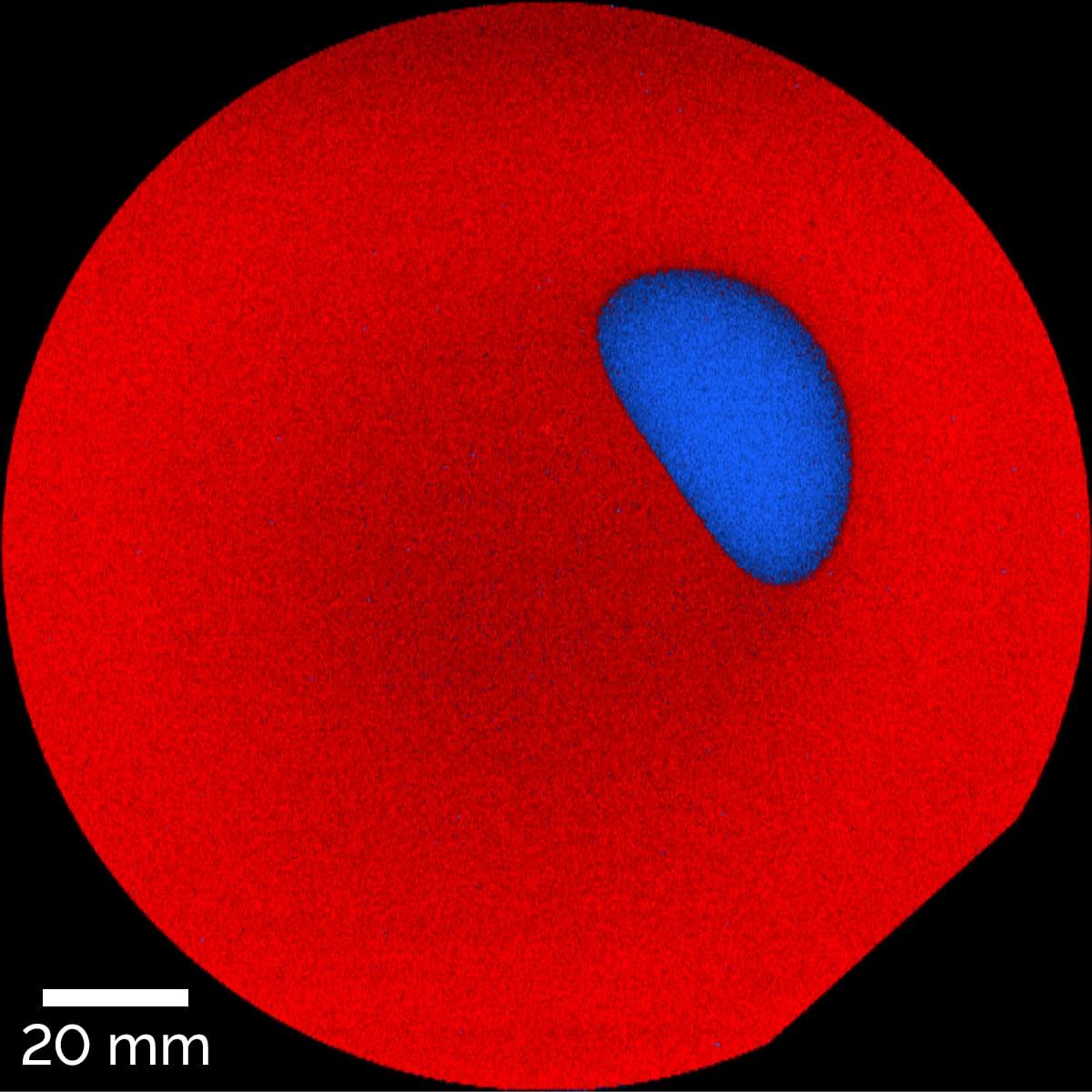
With the witec360 Semiconductor Edition, you can perform PL measurements to complement your Raman analyses. This is particularly interesting for investigating wide-bandgap semiconductors such as SiC or gallium nitride (GaN). The PL emission wavelength serves as an indicator for the material’s electronic properties, including its bandgap.
This PL image of a SiC wafer shows differences in PL properties, revealing defects. Read more in our application note: Correlative Raman Imaging of Compound Semiconductors
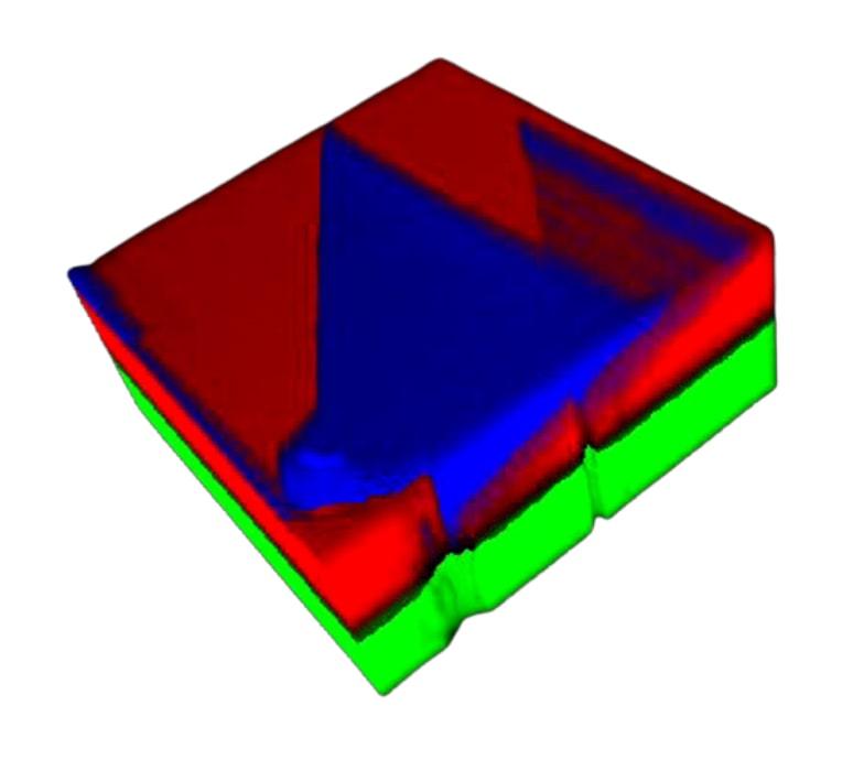
Raman imaging provides insight into the sub-surface properties of layered semiconducting materials. This depth scan through an epitaxially overgrown SiC wafer visualizes the distribution of its different layers.
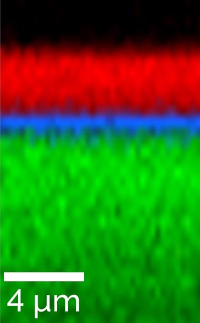
Sample courtesy of the Fraunhofer Institute for Integrated Systems and Device Technology IISB, Erlangen, Germany.
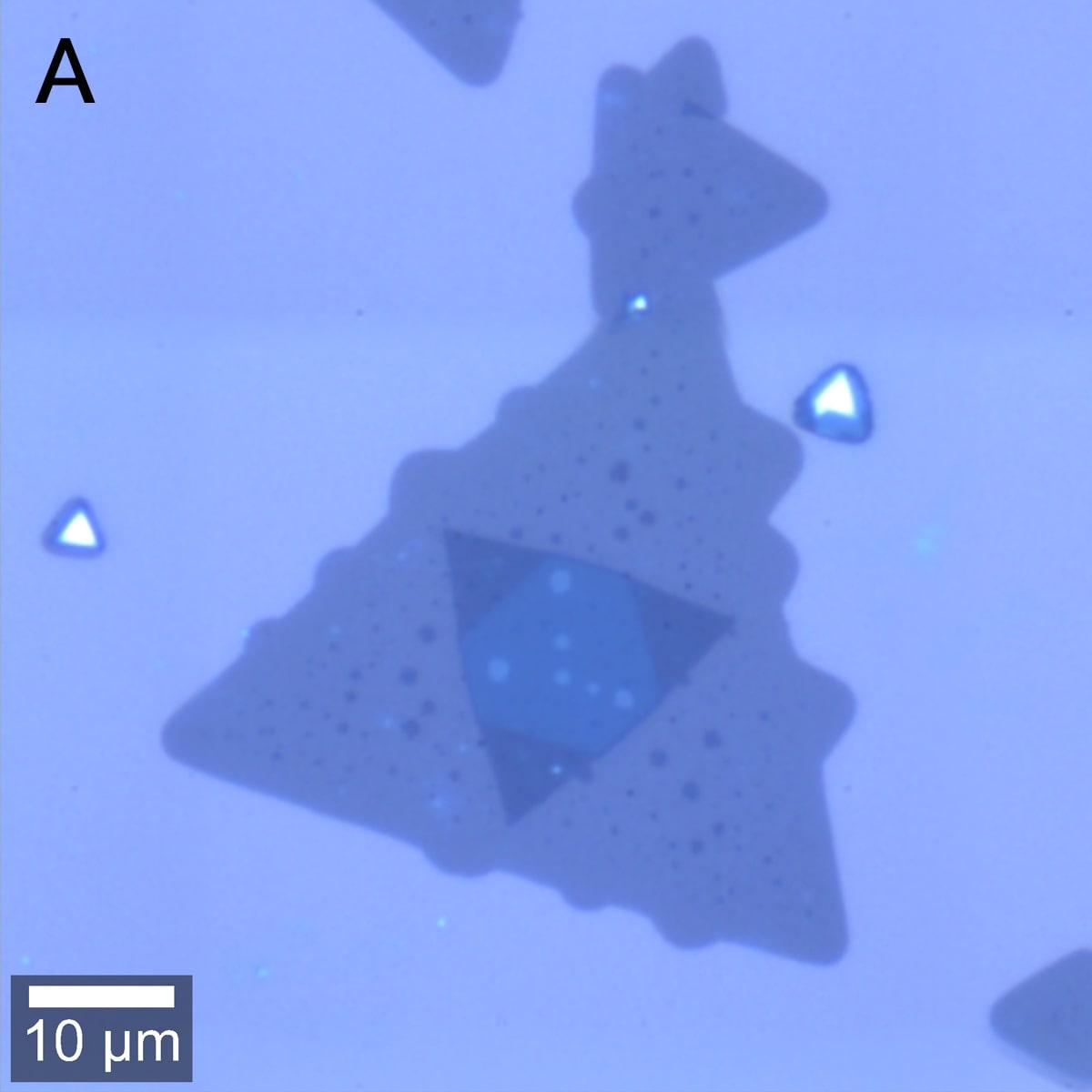
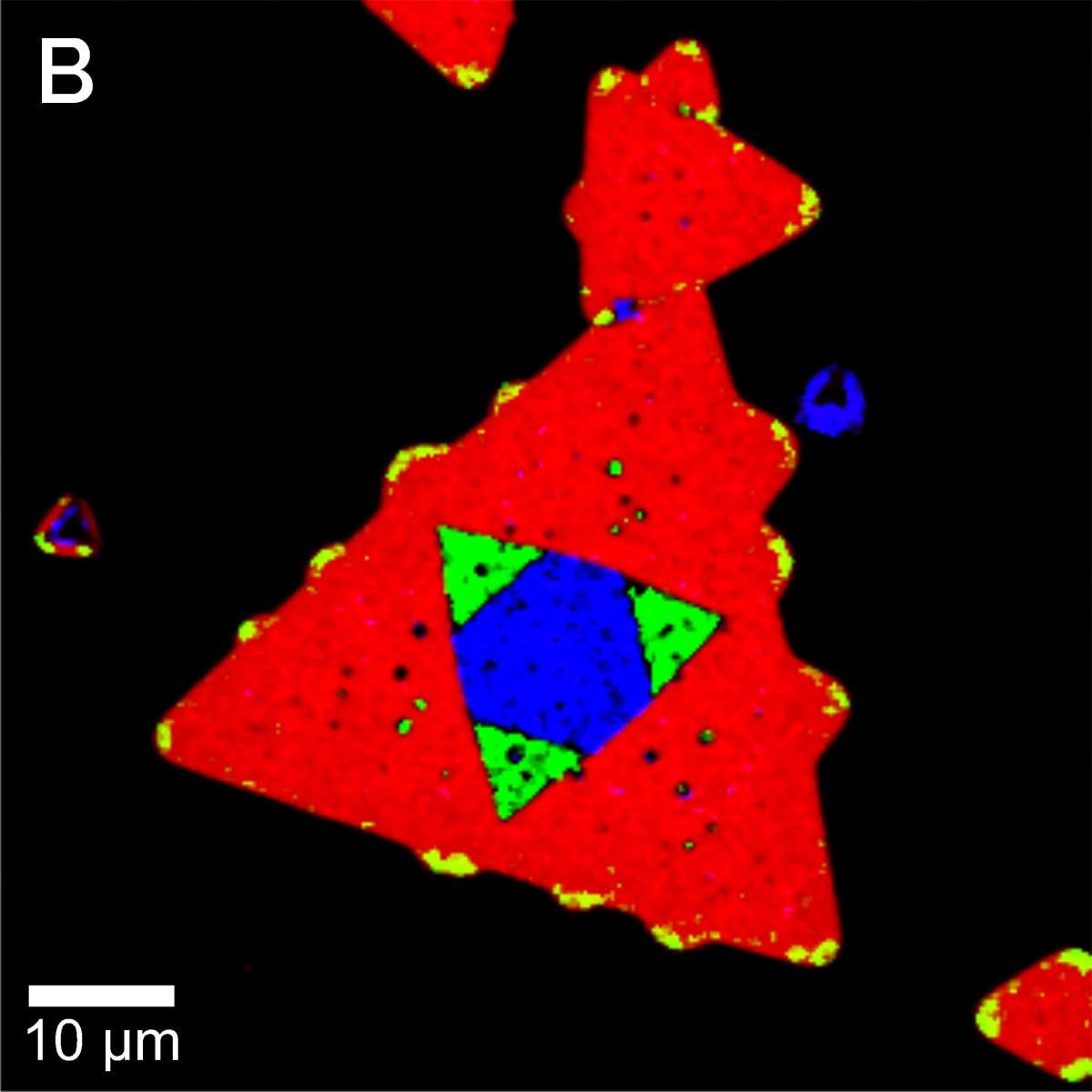
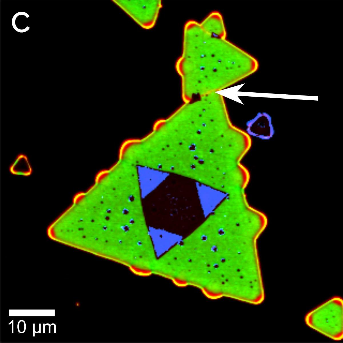
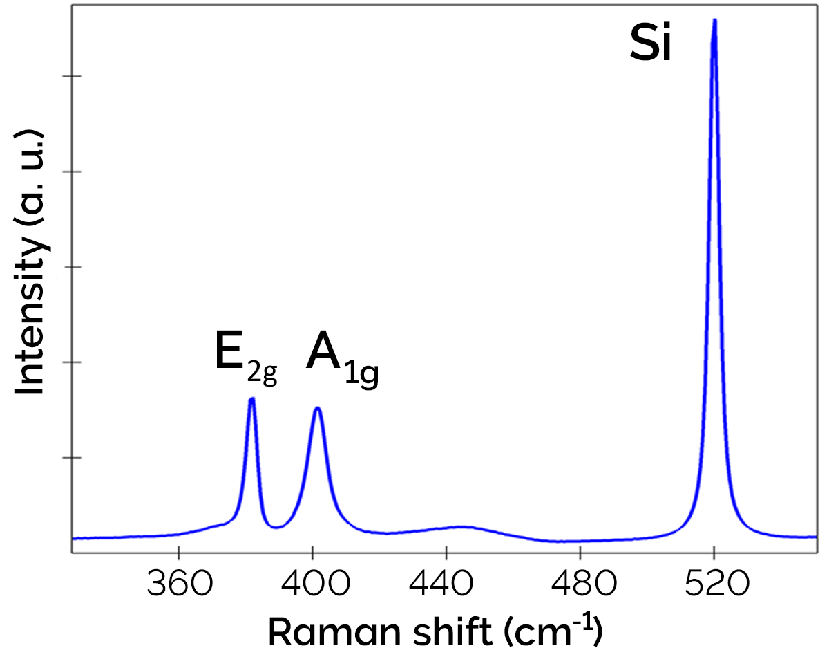
Novel 2D materials are of increasing interest for their unusual structural, electronic and optical properties. Correlative Raman imaging enables thorough characterization of these few- to single-layered materials, including graphene and perovskite, as well as molybdenum disulfide (MoS2), tungsten diselenide (WSe2) and other transition metal dichalcogenides (TMDs).
Learn more in our Application Notes:
Please fill in all data fields to ensure we can process your inquiry as quickly as possible.

© Oxford Instruments 2026
 Powered by Bioz