witec360 Raman microscope with Hexalight spectrometer launched
Take your research in any direction with the new benchmark for Raman imaging.
 Part of the Oxford Instruments Group

Semiconductors are the foundation of modern technologies, powering advancements in computing, telecommunications, energy, and optoelectronics. From transistors to photovoltaics and LEDs, these materials are at the core of countless devices. To meet growing demands for performance, efficiency, and reliability, precise characterization of semiconductor properties is essential at every stage, from research and development to production.
Confocal Raman microscopy and photoluminescence (PL) imaging are powerful techniques for semiconductor investigation, providing detailed insights into structural and electronic properties. These capabilities support quality assurance, optimize production processes, and accelerate time-to-market for new devices.
The Oxford Instruments witec360 microscopes are equipped to perform both state-of-the-art Raman and PL measurements in a single instrument, offering an advanced solution for the semiconductor field. Whether visualizing material uniformity or characterizing band gap properties, the witec360 empowers researchers and manufacturers to gain comprehensive material insights and overcome typical challenges in semiconductor innovation.
For whole-wafer access, discover our witec360 Semiconductor Edition, which is optimized for large-area imaging and accommodates wafers up to 12 inches (300 mm).
witec360 Semiconductor Edition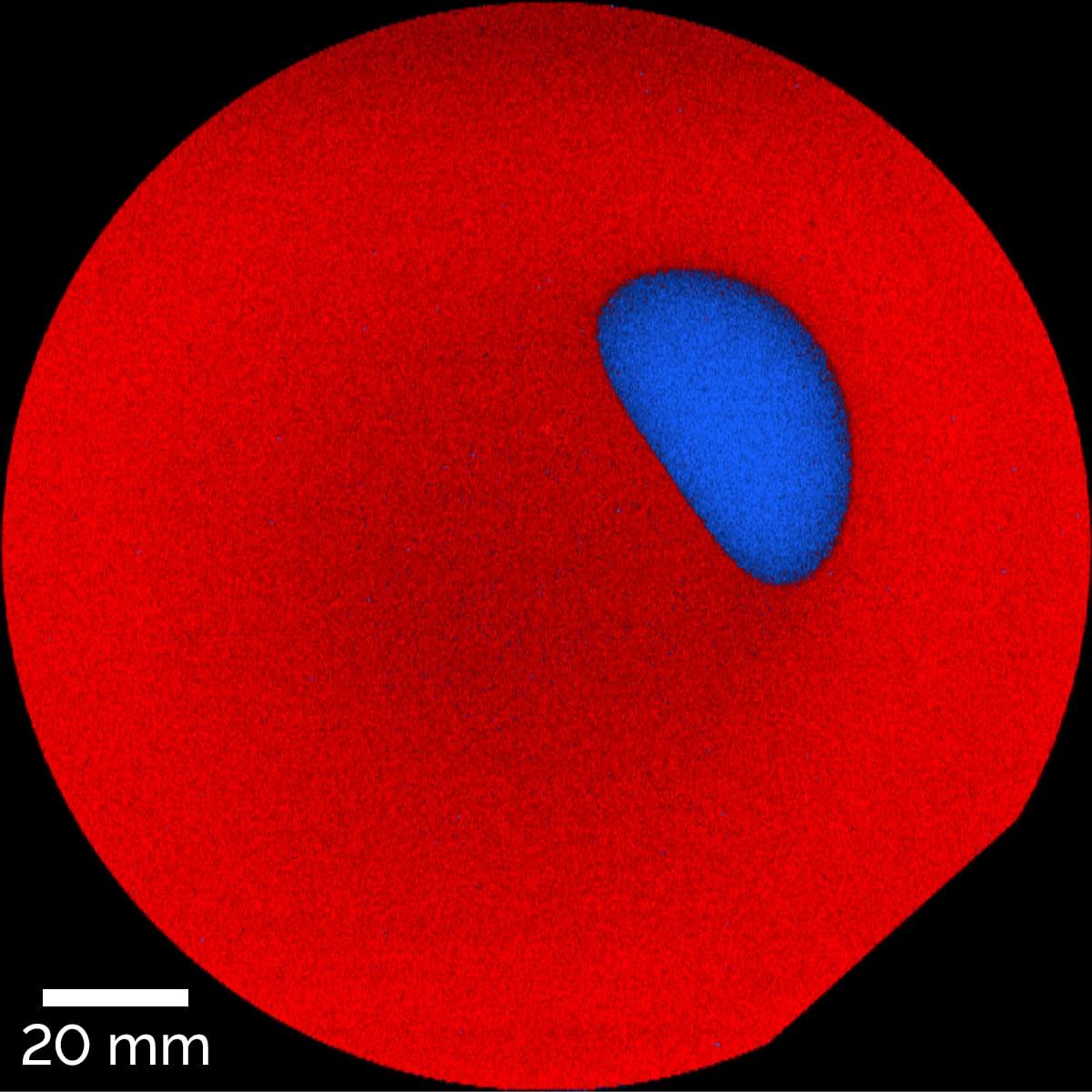
Raman and PL imaging are complementary techniques, ideally suited to be combined to provide researchers and manufacturers with the insights needed to optimize material properties and ensure the quality of final devices.
Explore our Application Note on Correlative Raman Imaging of Compound Semiconductors for a demonstration of correlative Raman-PL measurements in wafer analysis.
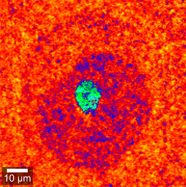
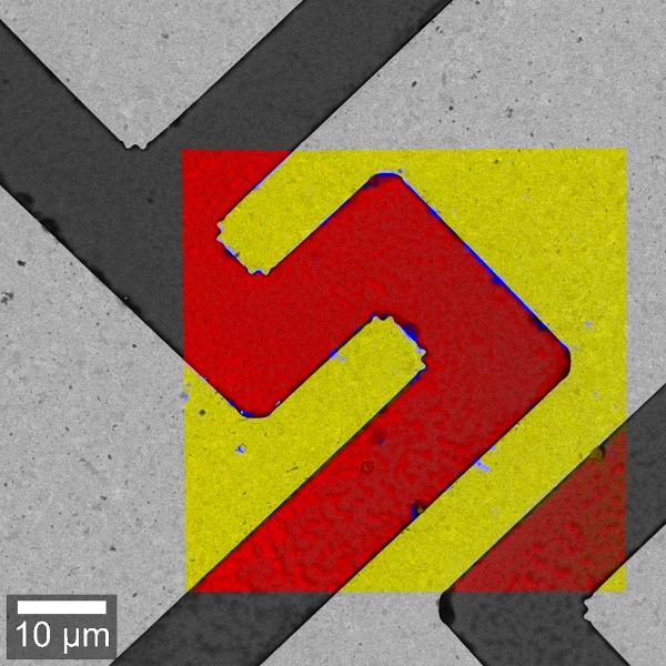
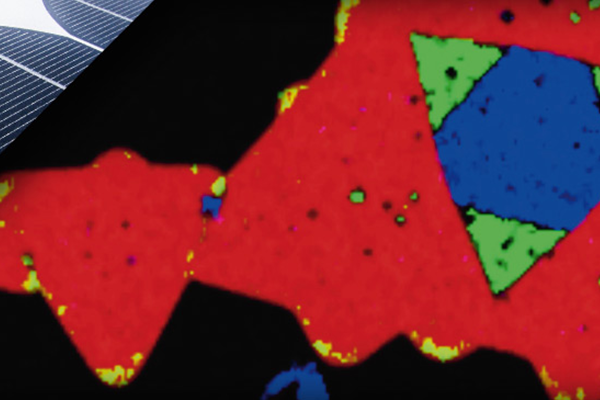
Minor changes in a semiconductor’s crystalline structure, such as those caused by stress or strain, can drastically influence its stability and electrical performance. The witec360 Raman microscopes deliver the exceptional sensitivity required to resolve even slightest Raman peak shifts, down to tenths and hundredths of a wavenumber. This is showcased here in Gallium Nitride (GaN), where we were able to identify tensile stress fields (blue and green coloured areas) induced by a Frank-Read source.
Read more about material stress analyses in our Application Note on Correlative Raman Imaging of Compound Semiconductors.
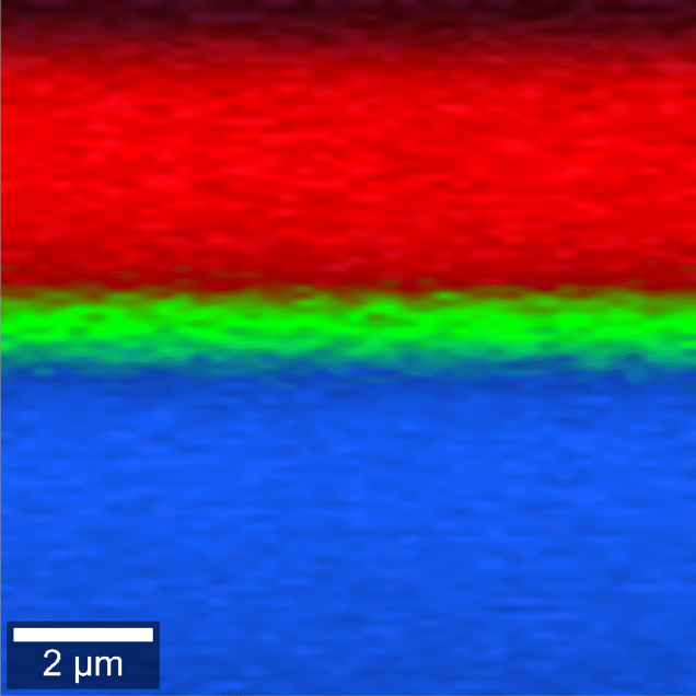
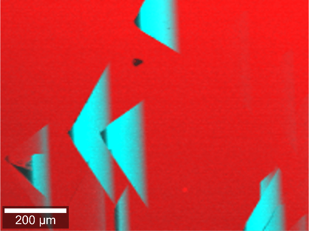
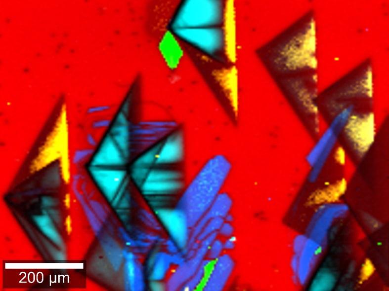
Confocal Raman microscopy enables non-destructive sub-surface structure analysis of semiconductor materials. Raman depth profiling the in xz-plane is ideal for determining doping profiles within a wafer and measuring layer thicknesses while maintaining sample integrity.
In this example, Raman depth profiling successfully resolved layers with differing doping concentrations in a processed 4H-SiC wafer: the substrate (blue), a 1 µm intermediate buffer layer (green), and a 9 µm epitaxial layer (red). The depth resolution required to accurately calculate the thickness of these layers was only possible due to the exceptional confocality in Oxford Instruments Raman microscopes.
Learn more in our Application Note on Correlative Raman Imaging of Compound Semiconductors.
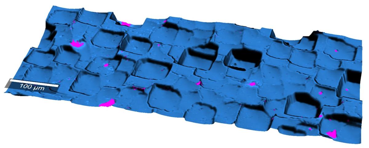
How can confocal Raman imaging maintain focus on a structured surfaces over long distances, such as in wafer imaging?
TrueSurface, our patented optical profilometer technology, provides the answer. It continuously adjusts the focus to the sample’s surface structure, maintaining exceptional focus stability in large-area imaging. TrueSurface also delivers detailed topographic information alongside measurement data in a single pass.
Combine Raman imaging with advanced analytical techniques to gain even deeper insights into your semiconductor’s properties. The correlative approach in Oxford Instruments Raman microscopes enables seamless integration of techniques to analyze chemical composition, electrical properties, topographic features, element distribution and to acquire high-resolution structural data. This allows for an comprehensive understanding that drives the optimization of semiconductor materials for cutting-edge applications.
Application Note Thermomechanical Raman Mapping
Application Note Compound Semiconductors
Application Note Semiconducting Materials
Application Note Group III Nitrides and 3D Raman
Application Note Solar Cells
If you'd like to learn more about the possibilities of Raman imaging for semiconductor and photovoltaic applications, one of our specialists will be happy to discuss them with you.
Contact us
© Oxford Instruments 2026